Daily Tech Briefing
AI 科技速览
每天 5 分钟内学习 AI。获取最新的人工智能新闻,理解其重要性,并学习如何将其应用于您的工作。
Hacker News · 2026/8/1 00:53:42
Looking inside a 1970s PROM chip that stores data in microscopic fuses (2019)
AI 中文解读
一块1970年代的老芯片藏着什么秘密?这次科技博主拆解了MMI 5300 PROM芯片,发现它用微小保险丝存储数据——完整代表1,烧断代表0,一次编程永久保存。当年这块芯片卖70美元,如今在显微镜下,1024位数据整齐排列成33×33的阵列,像是硅片上的微型熔断器迷宫。用今天的眼光看,这技术原始得可爱,但在当时却是只读存储的重要突破。普通人可能永远不会接触这种古董硬件,但理解它有助于明白一个基础道理:数据存储不只有硬盘和闪存,早期工程师靠烧断金属丝也能记录信息。这种“物理级”存储方式虽然笨拙,却奠定了可编程只读存储器的发展基础。看完这种拆解,你会感叹科技迭代的速度——现在一个指甲盖大小的芯片能存上千亿倍的数据,而几十年前,一块昂贵的芯片只能存放128个字母。技术就是这样,在不断的“烧断”与“重写”中向前奔跑。
The MMI 5300 was a memory chip from the early 1970s, storing 1024 bits in tiny fuses.1
Unlike regular RAM chips, this was
a PROM (Programmable Read-Only Memory);
you programmed it once by blowing fuses and then it held that data permanently.
The chip I examined originally cost $70 and was built by MMI (Monolithic Memories Incorporated), a leading PROM manufacturer at the time.
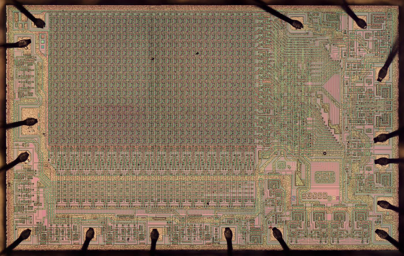
The highly magnified photo below shows the chip's silicon die.
The metal layer on top of the silicon is most visible in this photo; the transistors and resistors fabricated from
silicon are underneath.
The wires around the edges are the 16 bond wires between the silicon die and the external pins.
In the upper left, the
1024 bits of data are stored in a 33×33 array of diodes and fuses.
(I'll explain the extra row and column below.)
This chip is built from NPN transistors, unlike the MOS transistors used in most modern chips.
Die of the MMI 5300 PROM chip, holding 1024 bits of information. Click image for a larger version.
To produce the die photo, I started with the chips below, in their 16-pin ceramic packages;
the 5300 and 6300 chips are essentially the same.2
Since the chips were in ceramic packages, I could decap the chip simply by knocking the metal lid off with a chisel,
revealing the silicon die.
The MMI 5300 and 6300 PROM chips are in ceramic packages. The chips have 1974 and 1973 date codes.
In the photo below, the silicon die is mounted very off-center in the package. It's unclear if that is intentional or sloppy manufacturing.
Tiny bond wires connect the die to the metal contacts of the package.
The MMI 5300 PROM with the lid removed, exposing the die.
Inside the chip
The diagram below shows the main parts of the chip, with the pins labeled.
The chip stores 1024 bits as 256 4-bit words.
The 8 address lines A0-A7 select one of the 256 words, and the bits are output on pins Out1-Out4.
The Program pin is used to store data in the chip by blowing fuses.
The Vcc and ground pins power the chip.
Die of the 5300 PROM with components labeled.
The 1024 bits of data are stored in a 33×33 array of diodes and fuses.
Note that the data array only takes up about a quarter of the chip; the rest of the chip holds the supporting circuitry.
Below the data array, address decode circuitry used the address lines to select one of 32 columns in the array.
To the right, DTL multiplexers4 reduced the 32 rows of output to the 4 desired outputs. The output drivers amplified these signals and sent them to the output pins.
The fuses
The chip stored data in tiny fuses. An intact fuse represented a 1, while a blown fuse represented a 0.
Thus, the chip was shipped containing all 1's, and the user programmed the chip by blowing fuses where a 0 bit was
required.
The fuses were fabricated from tiny regions of Nichrome metal that heat up and melt under high voltage.
(Nichrome is a nickel-chromium alloy that has much higher resistance than typical metals, causing it to heat up.
It is commonly used in applications such as toasters.)
A closeup of the fuses (purple) that store data. Inset circle shows a magnified fuse, showing the tiny horizontal crack indicating the fuse was blown.
The fuses are visible in the die photo above; they are the purple regions between the metal wiring.
The fuses are very small, about 8µm long.
I expected a blown fuse would vaporize entirely, but instead a blown fuse contains a tiny crack roughly 700 nm wide.
(This is the wavelength of red light, so the crack is just barely visible under the microscope.)
Address decoding
The PROM stored 1024 bits as 256 words of 4 bits. However, the bits are physically arranged in a 33×33 grid since
a square memory grid is more efficient than a highly-rectangular one.
To access the memory, address bits A3-A7 select one of the 32 columns.
The selected 32 bits in the column go through the multiplexers at the right, which select one bit out of each group of eight,
based on address bits A0-A2. The four selected bits bec
分享
阅读原文 ↗